We’ll start with the myriad of tiny decisions made in a computer chip to gain some insight into the decisions we make throughout or lives
Tim Frodsham 30 October 2021
Decisions
This article will deviate from my usual genre but there is a purpose and a message in this. I am going to start by explaining the fundamental circuit a computer uses to make a decision. Rest assured, there is very little in here that is technical. In order to understand the explanations, you will need to spend some time pondering the pictures I have included, and even tracing the paths I describe to understand how the drawing works. It is not complicated, and my explanations will not require any technical or mathematical background. If you spend a bit of time in this article and familiarize yourself with the explanations, you will end up understanding how a computer does its thing better than 99% of the population. If you have no desire at all to talk even just a wee bit technical, then this is an article you may want to skip.
Electronics has revolutionized our lives, from the first days of electric motors and Edison’s light bulb to the sophisticated computer centric connected world of today. The first step in this electrical revolution was to harness electricity to do work: power motors to run our factories, ease our home life, and cook our food; pumps to deliver water and transport a myriad of products across town and around the world; and electrical energy to light our way.
The second stage of the electrical revolution was launched with the design of an electrical circuit capable of making a decision. Early on came simple electronic calculators. The first calculator I saw as a young college student could add, subtract, multiply, or divide two numbers and the most sophisticated could even find the square root of a number. These marvels of technology cost about the same as tuition for a full college semester. At about that time also came large room sized computers that could do thousands of calculations per second, followed by Mini computers, the personal computer, hand held computers, and mobile devices. All of this technology was and is enabled by a simple decision-making circuit with millions, and even billions, of them placed on an integrated circuit chip smaller than your thumbnail.
By the beginning of the 1990s, a Hallmark greeting card embedded with a microchip allowing it to play “Happy Birthday” contained more computing power than existed on the entire planet in the early 1950s (cs4fn.org). All of the information age technology around us is based on one simple circuit: a small set of transistors called a NAND gate that can examine information from two sources and make a single decision based on that information. The NAND gate has been implemented in numerous technologies and numerous ways, but the concept is the same. Don’t worry if you have no idea what NAND means, or what a transistor is, we will get to that later. There are several concepts you need to understand, and I cannot explain them all at once, so patience is in order. Hang in there, and this will make sense.
The decision that a NAND gate makes is tiny, akin to determining if, as you tossed a coin, you happened to toss two heads in a row. No big deal. In and of itself this is not much of a decision, and a far cry from heavy duty tasks such as Alexa trying to figure out what your 4-year-old is asking or complex simulations to determine the future weather. Some would argue that weather prediction is still pretty much a coin toss, but that’s another discussion. To perform these big-league tasks, all we need are lots and lots of little decisions—NAND gates that run in the millions and billions, each making their little decisions millions or billions of times a second. The basis of a computer chip is not some complex brain-like artificial being, but billions of these tiny, simple decision-making circuits which contribute each in a small way to the whole.
There are two major obstacles to designing and building modern computer chips. First, we have to be able to build billions of these chips cheaply and reliably. Integrated computer chips are made using a process similar to printing. In fact, one may reasonably call integrated circuit manufacturing the first application of 3D printing. Using modern lithographic type processes, millions of these computational machines can be pumped out of fabrication facilities, each containing the require billions of little decision-making circuits.
The second obstacle to building a computer chip is to organize the millions of these tiny decision-making circuits such that they work together in synchronous harmony to accomplish the tasks put before them. This is the epitome of a boot strap process. Powerful computers built using existing computer chip technology are used to run design and simulation tools to design, organize and verify even larger and more complex computer chips. Computers built with these more powerful chips are then used to run even more complex simulation and verification programs to design the next generation of chips. Generation by generation, powerful computers built with existing technology are used to design and build even more powerful computers. Decision making technology has exploded from the simple NAND gate, taking many complex forms using exotic technologies, but all can be traced back to this simple circuit.
To create this decision-making doo-dad, we first need a simple electronic switch, similar to the light switch on your wall. With the light switch off, power is cut off from the light fixture. With the switch on, power is connected and the light goes on. Simple. Wait, there’s a whole lot of stuff between the power plant and our homes, but at this point, I don’t care. Our focus is on the simple switch on the wall whose sole purpose is to connect or disconnect our lightbulb from the power in our home.

For our discussion here, we will look at the most ubiquitous technology used, called CMOS, or Complementary Metal-Oxide Semiconductor. Complementary meaning there are two types of switches in this technology which complement each other in function. The Metal-Oxide Semiconductor part is way beyond this article and you can simply ignore it. Maybe I’ll cover that one in a future essay…most likely not.
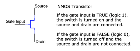
The first transistor in this pair is an NMOS (N-type Metal Oxide Semiconductor) transistor, the N referring to the type of physical element used in the manufacture of this device and not germane here. If we apply a logic one to the gate of this device, the switch turns on and the source is connected to the drain. If we apply a logic zero to the gate of this device, the switch turns off and breaks that connection. TRUE? FALSE? Logic 1? Logic 0? We’ll get to that in a moment.
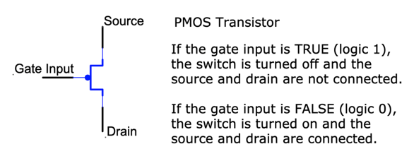
The complementary transistor is a PMOS (P-type Metal Oxide Semiconductor) device. If we apply a logic zero to the gate of this device, the switch turns on. If we apply a logic one to the gate, the switch turns off. Note that this is backwards from or complementary to the first device. What is important to understand here is we have a switch which we can turn on and off electrically.
Let’s talk a minute about what I mean by TRUE or logic 1, and FALSE or logic 0. These transistors are electronic switches, and work on an electrical voltage. The AAA battery you put in your television remote produces about 1.5 Volts. Not a lot, but enough to enable couch potato TV viewing. For our discussion here, let’s power our transistor circuits with 1 volt of electricity. A TRUE on the gate input of one of these devices means that we have applied 1 volt of electricity and call that a logic 1. A FALSE on the gate input means the application of 0 volts, and we call that a logic 0. These terms are interchangeable: TRUE, logic 1, or 1 volt mean the same thing in this circuit, as does FALSE, logic 0 or 0 volts. That’s all we get: TRUE or FALSE, logic 1 or logic 0.
A NAND gate in its most common form, the form we will learn about here, is made from four transistors. The implementation below uses CMOS transistors, but there are many other technologies that are used to make these decision-making elements. Before we move on, please note the little bubble in front of the PMOS transistor gate input. In circuit schematic jargon, the little bubble is used to denote a negative or inverse type function. In this case, it indicates that a PMOS transistor is turned on when the gate input is FALSE. The NMOS transistor has no such bubble, so we know that it is turned on when its gate input is TRUE. The NAND gate circuit below has two inputs, A and B, and one output: Out. We electrical engineers are so creative when it comes to names.
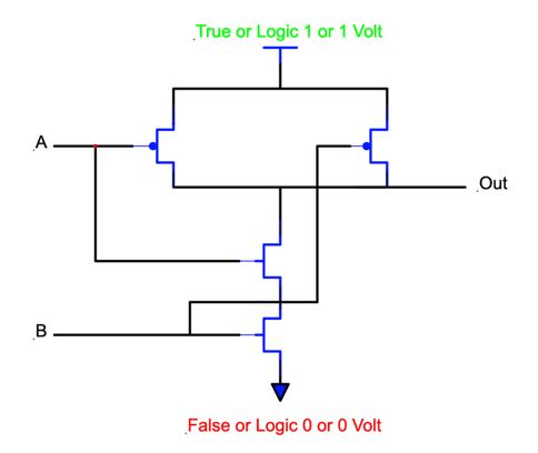
This diagram looks really messy, because connected my inputs to this circuit, A and B, to multiple points in the circuit. Drawing all the lines makes it hard to read, so I will simplify:
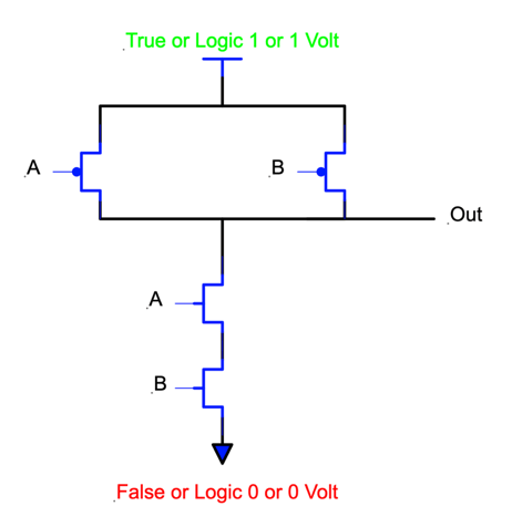
We have two inputs to this circuit: A and B. I have removed the lines, but A is hooked to one PMOS and one NMOS transistor, as is B. We have two PMOS transistors at the top of the circuit, and two NMOS transistors at the bottom. At the top of the drawing, the circuit is supplied with TRUE, or a voltage of 1. The bottom of the circuit is hooked to FALSE, or a voltage of zero. All of the black lines between the transistors are wires that hook these devices together. Let’s see how this doo-dad works.
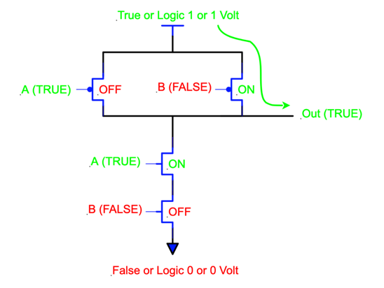
Through the B input of the PMOS transistors at the top of the circuit is supplied with a FALSE or logic 0, that transistor or switch is on, creating a path from TRUE to the output. Note that if the A input was FALSE, or if both of the inputs were FALSE, we would have the same result of TRUE routed to the output. Similarly, if either or both of the A and B inputs are FALSE, one or both of the bottom transistors are switched off, and the output is disconnected from FALSE. It takes only one of the NMOS transistors in the bottom to break the connection. Here is where I would like you to spend some time. Trace through the circuits. Print out the page and doodle on it with a pencil if that helps. As you are looking at these drawings, refer back to the description of each of the transistor types I included earlier. As you walk through this circuit, you should be able to convince yourself that if either or both of the inputs are FALSE, the output of this circuit is hooked to the TRUE symbol at the top of the drawing and disconnected from the false at the bottom.
Here is what happens when both inputs are TRUE:

Both of the top transistors are turned off, so the output is disconnected from TRUE. Both of the transistors in the bottom are turned on, so there is a connection, through the series combination of these switches, from FALSE to the output. (Series means that they are hooked up in a line, one on top of the other).
This is called a NAND gate. The output goes only FALSE if both inputs are TRUE. Back at our coin toss example, if you put on input A the results of the first coin toss, (TRUE meaning that you tossed a heads and FALSE if you tossed a tails) and the results of the second coin toss on input B, then the output would go FALSE only if both tosses were heads. Yes, I know, it seems backwards, one would think that the output would go TRUE if both coin tosses were heads, but that’s just how the circuit works. How we deal this negative logic is beyond the scope of this article. What is important is to understand that the output did something different if we had two-coin toss heads in a row. We were able to make a decision and that is all we need.
The function we have described is a NAND function. Only if input A AND input B are TRUE does the output go FALSE. The ‘N’ in NAND gate means that the logic is negative. If the input criteria are met, the output goes FALSE, otherwise it is TRUE: backwards or ‘Negative’ from what we would expect from an AND gate. The TRUE or FALSE output from this NAND gate can be used as the input for other NAND gates along the way. In this way, we can combine a whole bunch of these gates to make more and more complex decisions.

This symbol is widely used to represent the NAND function and simply means the circuit with four transistors we just discussed above. Note again the little bubble, this time on the output. This means that when the input criteria are met, we get a FALSE on the output, not a TRUE. That’s it. Once we have an electronic circuit that can make a decision, we can now use a bunch of these to make more and more complex decisions and functions, like adding numbers together, checking the grammar on your writing assignment, help to determine just what you want to purchase on Amazon, or attempting to figure out why your bank account is overdrawn. How we do this is the second major task in computer chip design. This involves arranging and connecting millions of these decision-making gates in just the right way, and then controlling the flow of decisions from one place in the chip to the next. Writing apps or programs to make a computer more versatile is important and complicated, but not germane to the discussion here, and besides, I’m an electronics engineer…not really interested.
Harnessing this decision-making capability in a computer is achieved by breaking down the overall decision-making process into little time intervals. At the beginning of the interval, information flows from one NAND gate to the next, decisions made on the way. At the end of the interval, decisions made by the end of this cycle are captured and held for the beginning of the next cycle and the next stage of decision making. It turns out that these little memory devices, doo-dads that hold these results from one cycle to the next are also made out of . . . NAND gates, but that is for another essay. Exactly how we design and control this flow of information and decision making requires the design talents of hundreds or even thousands of engineers and is way beyond the scope of this little essay. Even at this point you now know more about how a computer works than 99% of your friends and family.
I am normally not a big fan of analogies, and I use them sparingly. They tend to break down quickly and cause more dissension them discussion. In this case, it was writing about the decision-making process in computers that drew me to think about the decision-making process in our own lives. Learning to make decisions is at the foundation of this existence. Our second estate, agency, opposition, trials and common weaknesses all form an environment in which we need to choose. Making decisions is a part and parcel of every day existence and we make an uncountable number of little decisions every day: yellow light, Hmmm, should I speed through? Agency and the opportunity to make decisions are synonymous. It is it is not necessarily one major decision, but the myriad of small seemingly insignificant decisions and how we control them that shape this mortal existence.
Where this analogy breaks down to me is significant, and why I decided to use it. In a computer, there is no room for error. Though the contribution of each NAND gate is tiny, it is also crucial. One misfunctioning NAND gate can cause the whole chip to fail and be discarded. A wrong decision anywhere in the complex connection of decision-making circuits may lead to anomalous and incorrect results. Countless dollars are spent making sure that the computer chips in your phone, your computer or your car are as flawless as possible. If a computer chip makes mistakes, we discard it. For us there is recourse for bad decisions, which is the Atonement of our Lord and Savior Jesus Christ.
Unlike our expectations of the computer, Jesus Christ does not expect our decisions to be perfect. This earth life is designed to surround us with an onslaught of difficult situations and seemingly impossible choices: race, morality, gender equality, poverty, LGBT questions in light of the proclamation on the family, marriage, family, war, natural and man-made disasters… Add your favorite insurmountable obstacle here. And yes, you can even add that yellow light. We make imperfect decisions all the time, it’s part of the plan. Through His atonement, we can recover from these mistakes, learn the most important of life’s lessons and move forward in obedience to our Savior. I heard a quote somewhere, and cannot remember the source: “We do not earn or way to exaltation, we learn our way”. It is not a matter of how many times we get it wrong, or even how many times we get it right, but the direction of our progress, one tiny decision at a time.
